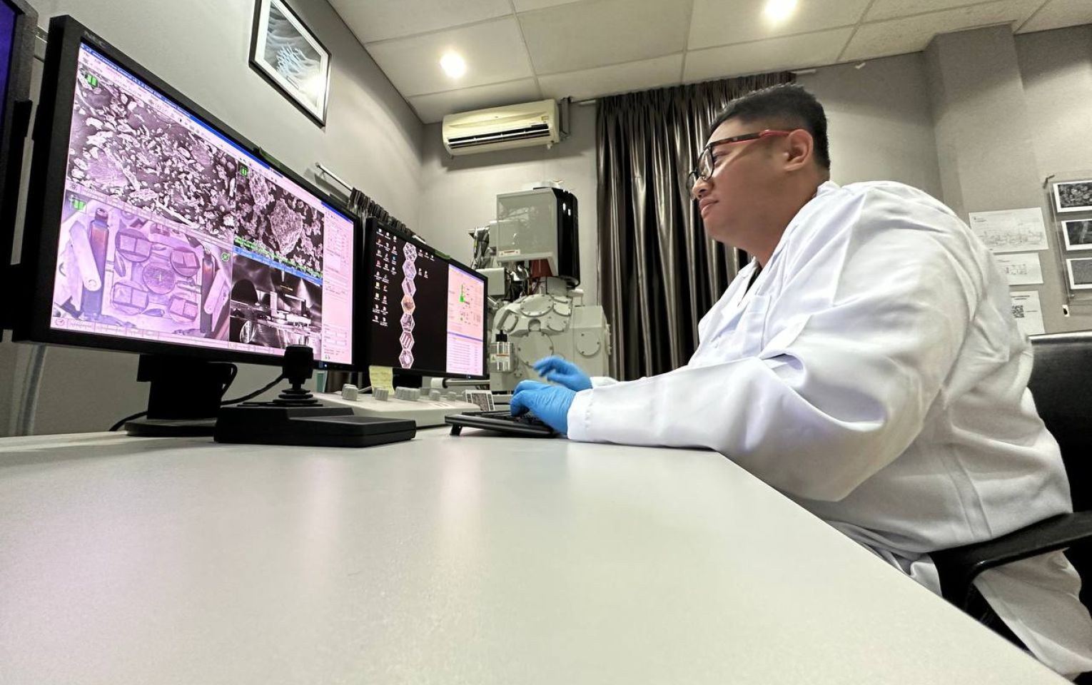
EXTREME HIGH RESOLUTION FIELD EMISSION SCANNING ELECTRON MICROSCOPE (XHR-FESEM) with Energy Dispersive Spectroscopy (EDS)
DOWNLOAD REQUEST FORM HERE
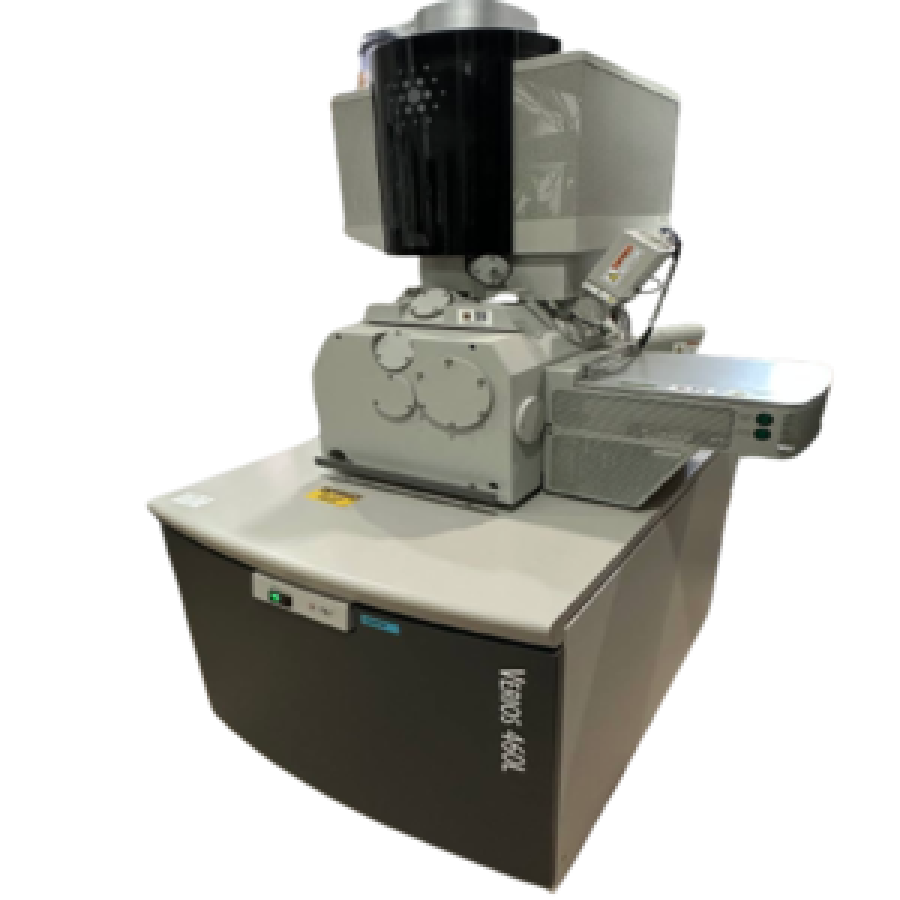
INSTRUMENT NAME & MODEL: Extreme High-Resolution Field Emission Scanning Electron Microscope (XHR-FESEM) Model FEI Verios 460L
Experience Unmatched Imaging with Field Emission Scanning Electron Microscopy (FESEM)
Discover the unparalleled capabilities of Field Emission Scanning Electron Microscopy (FESEM), delivering topographical and elemental insights at magnifications ranging from 100x to an astonishing 1,000,000x, all while maintaining virtually unlimited depth of field. Compared to conventional Scanning Electron Microscopy (SEM), FESEM offers significantly clearer and less electrostatically distorted images with spatial resolution down to an impressive 1.5 nanometers—three to six times better than traditional SEM.
Why Choose FESEM?
- Enhanced Contamination Detection: Examine smaller-area contamination spots at electron-accelerating voltages compatible with Energy Dispersive Spectroscopy (EDS).
- Surface Precision: Reduced penetration of low-kinetic-energy electron probes allows for closer examination of the immediate material surface.
- Superior Imaging Quality: Achieve high-quality, low-voltage images with negligible electrical charging of samples, operating at accelerating voltages from 0.5 to 30 kilovolts.
- No Conducting Coatings Needed: Eliminate the need for placing conducting coatings on insulating materials.
For ultra-high-magnification imaging, our advanced In-Lens FESEM takes your analysis to the next level. In-Lens FESEM provides topographical details at magnifications from 2000x to an astounding 1,000,000x, maintaining virtually unlimited depth of field. This state-of-the-art technology delivers images with even greater clarity and minimal electrostatic distortion, achieving spatial resolution down to an extraordinary 0.6 nanometers—three times better than regular FESEM and ten times better than conventional SEM.
CATEGORY: ELECTRON MICROSCOPE LABORATORY
SPECIAL FEATURES
- Electron beam resolution:
Resolution @ optimum WD- 6 nm at 30 kV (STEM *)
- 7 nm at 15 kV
- 7 nm at 1 kV
- nm at 500 V (ICD **)
- 2 nm at 200 V (ICD **)
- Landing energy range
- 20 eV - 30 keV
- Probe current
- E-beam: 0.8 pA up to 100 nA
- Detectors
- In-lens SE detector (TLD-SE)
- In-lens BSE detector (TLD-BSE)
- In-column SE detector (ICD) **
- In-column BSE detector (MD) **
- Everhart-Thornley SE detector (ETD)
- IR camera for viewing sample/column
- Chamber mounted Navigation Camera
- Retractable low voltage, high contrast solid-state backscatter electron detector (DBS)
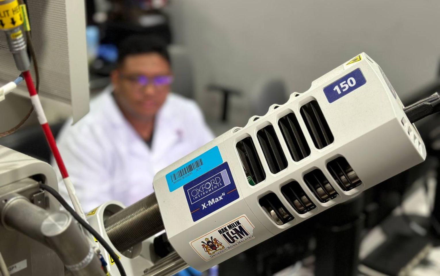
- Oxford Silicon Drift Detector (SDD) - X-Max EDS/EDX detector
- Sample sizes
- Maximum size: 0.5cm
- Maximum size: 1cm (Mold sample)
- Maximum sample thickness (via load lock/chamber door): 19 mm incl. stub
- Weight: 200 g (incl. holder)
- Sample holders
- Multi-stub holder (5 stubs)
- Multi-sample cross-sectional holder
- Single stub mount, mounts directly onto stage
- Various wafer and custom holder(s) available by request
Application
-
Our advanced instrumentation is ideal for a wide range of scientific and industrial applications, providing unparalleled insights into the morphological, chemical, and analytical properties of various materials. Key applications include:
- Material Characterization
Obtain detailed information on the morphology and composition of biological (dry samples only), polymeric, metallic, and composite materials.
- Failure Analysis
Identify the root causes of material failure in diverse industries, from aerospace to automotive.
- Geological Exploration
Conduct precise mineralogical and petrological studies to support resource exploration and extraction.
- Biological Studies
Analyze the structural and compositional properties of biological samples, enhancing research in fields such as medicine and biotechnology.
- Nanotechnology Research
Explore the nanoscale properties of materials, driving innovation in nanomaterials and Nano devices.
- Environmental Analysis
Perform detailed analyses of environmental samples to monitor pollution and study ecological impacts.
- Materials Development
Accelerate the development of new materials with advanced characterization techniques.
- Art Conservation
Support the preservation and restoration of artworks with precise imaging and elemental analysis.
- Semiconductor Quality Control
Ensure the highest standards in semiconductor manufacturing through rigorous quality control processes.
- Microscopy and Analytical Imaging: Utilize high-resolution imaging for comprehensive material analysis.
- Adhesion, Bonding, and Coating: Investigate and optimize surface treatments and coatings for improved performance.
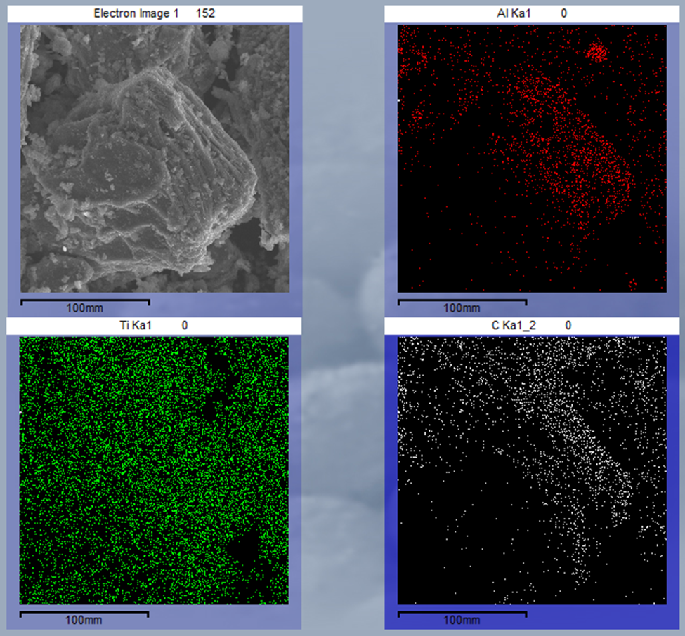
- Chemical and Elemental Mapping
Generate detailed maps of elemental distribution within samples for in-depth chemical analysis.
- Contamination Analysis
Detect and analyze contaminants to ensure the purity and quality of materials.
- Material/Nanomaterials Characterization
Characterize materials at the nanoscale for advanced research and development.

Sample Requirements
-
Our instrumentation supports a variety of sample types to meet diverse research needs:
- Powder or Solid Samples: Ideal for bulk material analysis and characterization.
- Film Samples: Perfect for examining thin films and coatings.
- Dry and Non-Magnetic Samples: Suitable for a wide range of applications, ensuring accurate results without interference.
Typical Results
Typical Results FESEM
FESEM SPECTRUM EDX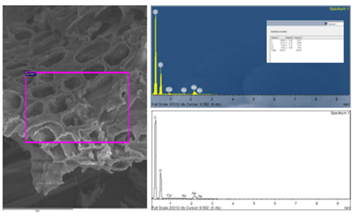
SEM MAPPING
