HRTEM-High Resolution Transmission Electron Microscope
DOWNLOAD REQUEST FORM HERE
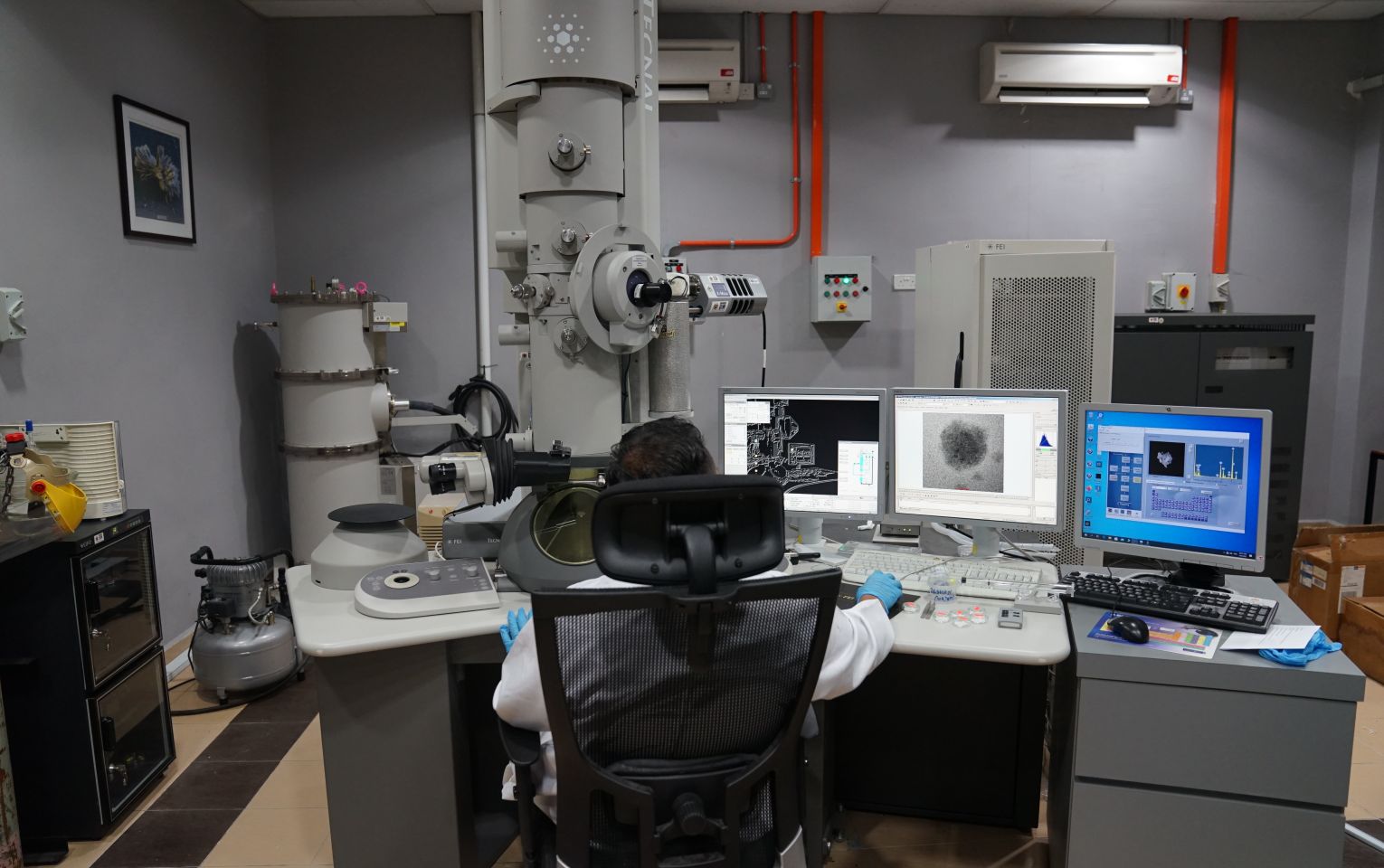
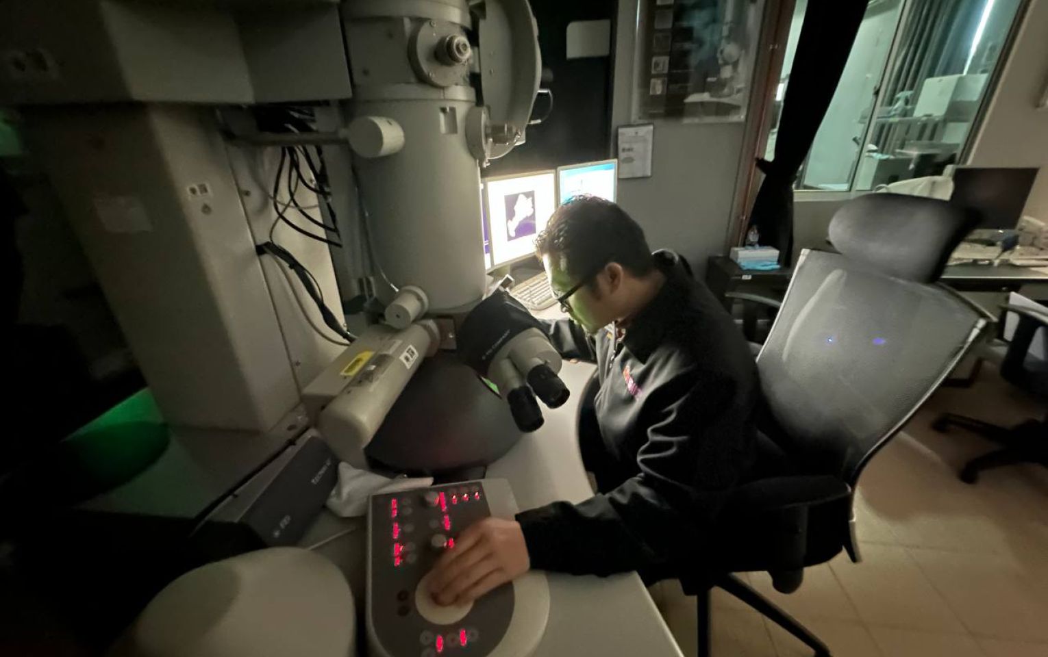
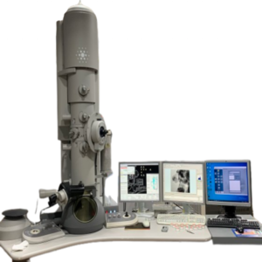
Instrument Name & Model: High Resolution Transmission Electron Microscope (HRTEM) 200kV with Field Emission, TECNAI G2 20 S-TWIN, FEI
The High Resolution Transmission Electron Microscope (HRTEM) is a state-of-the-art analytical tool that allows atomic-level insights into the structure, morphology, and crystallographic properties of materials. Specifically, the FEI TECNAI G2 F20 system provides exceptional high-resolution imaging capabilities with a point-to-point resolution of 0.2 nanometers, enabling detailed visualization of atomic arrangements within a material. In general, a HRTEM can:
- Capture the image morphology of samples, e.g., view sections of material, fine powders suspended on a thin film, and small whole organisms such as viruses or bacteria
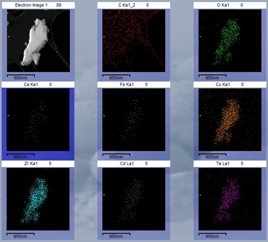
- Generate characteristic X-rays from samples for elemental analysis.
- Acquire electron diffraction patterns.
CATEGORY: ELECTRON MICROSCOPE LABORATORY
Special Features
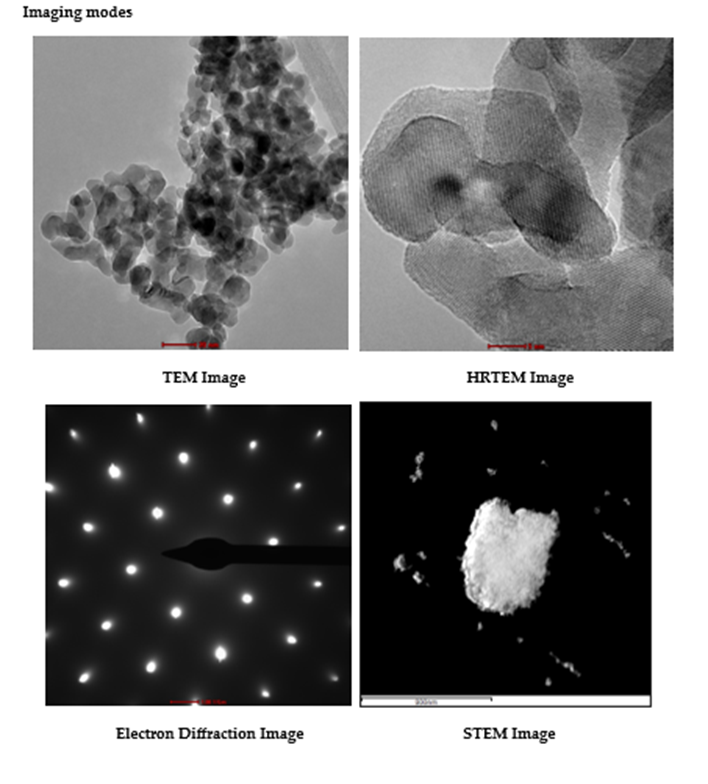
- TEM and HRTEM imaging
- STEM imaging
- Electron diffraction (SAED, CBED)
- Low background double tilt holder for EDX analysis
- Oxford EDX SDD Detector 80 mm2
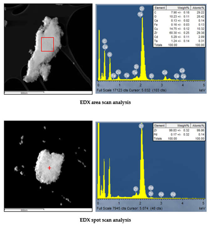
- Oxford EDX mapping, point, area, and line scan elemental analyses
- Excellent stability of focus, high tension, energy spread, spot, and alignment
- Complete and fast recall of all modes and accelerating voltage settings
- Full digital control of STEM/TEM and accessories.
Applications
-
TEM Applications
- Material Science: Characterization of the microstructure, crystal defects, phase distribution, and grain boundaries of metals, alloys, ceramics, and composites. It helps to understand the material properties that influence mechanical strength, corrosion resistance, and electrical properties.
- Nanotechnology: Characterization of the nanoparticles' size, shape, distribution, and aggregation state. It is critical for applications in drug delivery, catalysis, and the nanostructured materials development.
- Chemistry: Characterization of the morphology and structural details of chemical compounds, including catalysts, is pivotal in the development of new chemical processes and materials.
- Semiconductor Industry: Analysis of semiconductor devices, allowing for the visualization of junctions, interfaces, and layers at high resolutions, is crucial for device development and failure analysis.
- Biology: Characterization of the ultrastructure of cells, viruses, and subcellular components. It provides detailed images of organelles, including mitochondria, vesicles, and the complex structures within the cell nucleus.
HRTEM Applications
- Atomic-Scale Imaging: Imaging atomic arrangements in crystals, enabling the study of crystal structures, lattice spacings, and defect analysis such as dislocations, vacancies, and interstitials.
- Phase Identification: Provide detailed images at the atomic scale, HRTEM helps identify different phases within materials, especially those that are too fine to be resolved by other techniques.
- Interface and Boundary Analysis: Examine the characteristics of grain boundaries and interfaces between different materials, which are vital in understanding the properties of composites and multi-layered structures.
- Quantitative Measurement: Precise measurements of interplanar spacings and to quantify the degree of crystallinity or the presence of amorphous regions within a sample.
- Nanostructure Evaluation: Characterization of nanostructures, including quantum dots, nanowires, nanotubes, and graphene layers, providing insights into their structural perfection and defects.
Sample Requirements
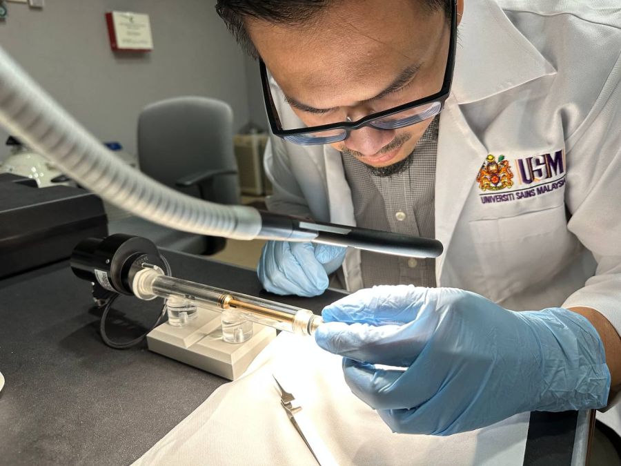
- Powder
- Thin film
- Solid
- Liquid/solution
- FIB lamella
Typical Results
HRTEM Typical Results
TEM MAPPING
TEM SPECTRUM
